[PDF] Intro to PCB Design: A Beginner’s Guide to Mastering PCB Layout! Pcb board design guide at santiago vanmatre blog
Delving into the fascinating world of PCB assembly, it's easy to get lost in the intricate details of soldering techniques and signal integrity. Let's explore two essential elements: reflow soldering and impedance control, both crucial for creating reliable and high-performance electronic devices.
Reflow Soldering: Mastering PCB Assembly Techniques

Reflow soldering is the cornerstone of modern surface mount technology (SMT). Unlike hand soldering, which involves individually soldering each component, reflow soldering is a bulk process that allows for the simultaneous attachment of numerous components to a PCB. It all begins with applying solder paste to the board, usually through a stencil. This paste contains solder particles, flux, and a binding agent, holding the components in place until the soldering process. Then comes the magic: the PCB is passed through a reflow oven, where it is subjected to a carefully controlled temperature profile. This profile typically consists of preheating, thermal soak, reflow, and cooling stages. During the preheating stage, the PCB and components are gradually brought up to temperature, preventing thermal shock. The thermal soak stage allows the temperature to stabilize across the entire board, ensuring uniform heating. The reflow stage is where the solder melts and forms a metallurgical bond between the component leads and the PCB pads. Finally, the cooling stage allows the solder to solidify, completing the connection.
Achieving a successful reflow soldering process requires careful attention to detail. The temperature profile must be optimized for the specific solder paste and components being used. Insufficient heating can result in cold solder joints, which are weak and unreliable. Excessive heating can damage components or cause the PCB to delaminate. Furthermore, the placement of components must be accurate to ensure proper alignment with the solder pads. Factors like humidity and air flow within the reflow oven can also influence the outcome, and should be carefully controlled. With a well-executed reflow soldering process, you can achieve high-quality, reliable solder joints that are essential for the performance and longevity of electronic devices.
Mastering PCB Impedance Control: Key Concepts for 2024
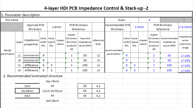
In the realm of high-speed digital circuits, impedance control is no longer a nice-to-have; it's an absolute necessity. Impedance control refers to the process of maintaining a consistent characteristic impedance along the signal traces of a PCB. Why is this so important? Well, when signals travel at high speeds, they behave like waves, and any impedance mismatch can cause reflections. These reflections can distort the signal, leading to timing errors, reduced signal integrity, and ultimately, system malfunction. Imagine shouting in a canyon: the echo is a reflection of your voice. Signal reflections are similar, but much more problematic in electronic circuits.
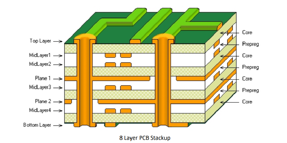
Several factors influence the impedance of a PCB trace, including the trace width, trace thickness, dielectric constant of the PCB material, and the distance to the ground plane or power plane. By carefully controlling these parameters during the PCB design and fabrication process, engineers can achieve the desired impedance. For example, increasing the trace width generally decreases the impedance, while increasing the distance to the ground plane increases the impedance. Specialized software tools are used to simulate and calculate the impedance of different trace configurations. Impedance control is particularly critical in applications involving high-speed data transmission, such as networking equipment, computer motherboards, and telecommunications systems. As data rates continue to increase, the need for precise impedance control will only become more paramount.
Furthermore, the choice of PCB materials plays a significant role. Materials with lower dielectric constants and lower loss tangents are preferred for high-speed applications, as they minimize signal attenuation and distortion. Manufacturers often use controlled impedance PCB fabrication techniques, which involve precise etching, layer registration, and material selection to ensure that the impedance specifications are met. Testing and verification are also crucial to confirm that the fabricated PCBs meet the required impedance tolerances. This is often done using time-domain reflectometry (TDR), which sends a pulse down the trace and measures the reflections to determine the impedance profile. In conclusion, mastering both reflow soldering and impedance control are key to building reliable and high-performing electronics, especially in the ever-evolving landscape of technology.
If you are searching about Mastering Unit Conversion in PCB Layout: A Definitive Guide to you've visit to the right place. We have 25 Pictures about Mastering Unit Conversion in PCB Layout: A Definitive Guide to like Mastering EMI Suppression: Effective Strategies in PCB Layout Design, Mastering Signal Tracing: Essential Rules for PCB Layout Design - 86PCB and also PCB design: Typical layout characteristics - JPE. Read more:
Mastering Unit Conversion In PCB Layout: A Definitive Guide To
 www.raypcb.com
 Mastering Unit Conversion In PCB Layout: A Definitive Guide To
 www.raypcb.com
 Reflow Soldering: Mastering PCB Assembly Techniques
reprosupplies.co.za Mastering Signal Tracing: Essential Rules For PCB Layout Design - 86PCB
 86pcb.com
 PCB Stackup Design Guidelines - MOKO Technology
 www.mokotechnology.com
 Pcb Board Design Guide At Santiago Vanmatre Blog
 storage.googleapis.com
 Mastering PCB Impedance: The Often-Neglected Key To Perfect Design : R
 www.reddit.com
 Mastering PCB Layout Design Rules For Optimal Circuit Performance - 86PCB
 86pcb.com
 How To Design A PCB Layout: A Comprehensive Guide
 www.wevolver.com
 PCB Layout Optimization For EMI And EMC
 pcbmust.com
 High Speed Pcb Layout Guidelines - Design Talk
 design.udlvirtual.edu.pe
 Mastering EMI Suppression: Effective Strategies In PCB Layout Design
 86pcb.com
 Mastering PCB Heat Dissipation - IBe Laser Vietnam - PCB & PCB Assembly
 en.ibe.com.vn
 Complete Guide To PCB Design For Beginners | PCB Tool Expert
 pcbtoolexpert.com
 A Detailed Guide To PCB Layout Design |Qtech Technology Co. Ltd
 qtech-us.com
 PCB Design: Typical Layout Characteristics - JPE
 www.jpe-innovations.com
 pcb design layout typical width trace mm characteristics jpe thickness minimal recomm
Mastering PCB Design Fundamentals - White Paper
 www.allaboutcircuits.com
 Mastering PCB Impedance Control: Key Concepts For 2024
 www.pcbonline.com
 PCB Layout Support - Embizon Technologies - PCB Design Services, Bangalore
 www.embizon.com
 Mastering PCB Impedance Control: Key Concepts For 2024
www.pcbonline.com Mastering The Art Of PCB Design Basics | Sierra Circuits
 www.protoexpress.com
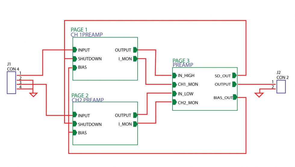
 pcb schematic mastering
Mastering The Art Of PCB Design Basics | Sierra Circuits
 www.protoexpress.com
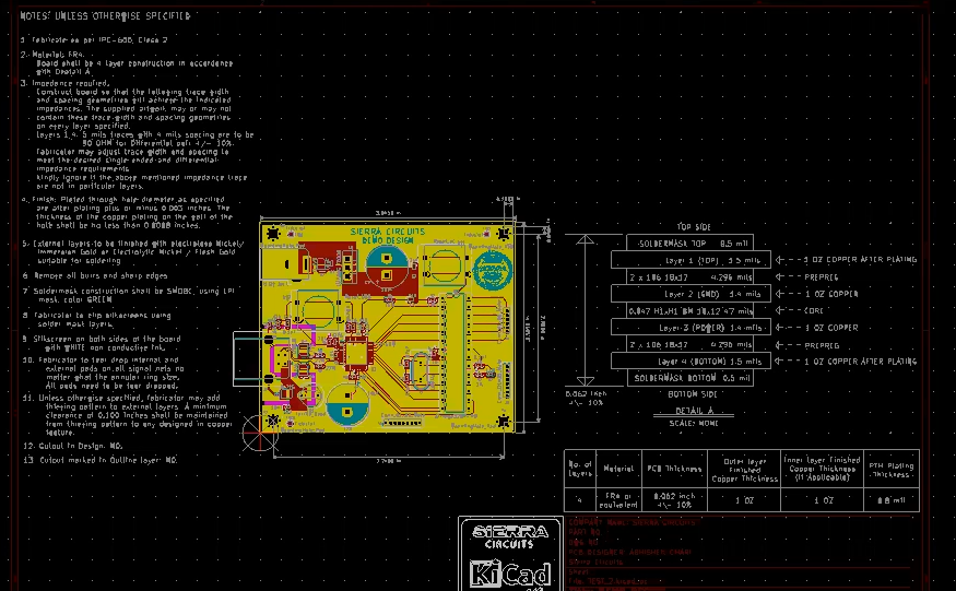
 pcb fabrication basics mastering
(PDF) Intro PCB Design Rev1 - DOKUMEN.TIPS
 dokumen.tips
 Mastering The Art Of PCB Design Basics | Sierra Circuits
 www.protoexpress.com
 pcb mastering
Pcb Design Using Ai Free Pcb Schematic Entry & Layout Software Beat
 pcbways.pages.dev
 Mastering signal tracing: essential rules for pcb layout design. Mastering emi suppression: effective strategies in pcb layout design. Mastering the art of pcb design basics